- 您现在的位置:买卖IC网 > Sheet目录1214 > EVAL-ADE7953EBZ (Analog Devices Inc)BOARD EVAL FOR ADE7953
�� �
�
�Data� Sheet�
�I� 2� C� INTERFACE�
�The� ADE7953� supports� a� fully� licensed� I� 2� C� interface.� The� I� 2� C�
�interface� operates� as� a� slave� and� uses� two� shared� pins:� SDA� and�
�SCL.� The� SDA� pin� is� a� bidirectional� input/output� pin,� and� the�
�SCL� pin� is� the� serial� clock.� Both� pins� are� shared� with� the� SPI�
�and� UART� interfaces.� The� I� 2� C� interface� operates� at� a� maximum�
�serial� clock� frequency� of� 400� kHz.�
�The� two� pins� used� for� data� transfer—SDA� and� SCL—are�
�configured� in� a� wire-AND� format� that� allows� arbitration� in�
�a� multimaster� system.� Note� that� the� ADE7953� requires� a�
�minimum� delay� of� 100� ns� between� the� SCL� and� SDA� edges,�
��Communication� via� the� I� 2� C� interface� is� initiated� by� the� master�
�device� generating� a� start� condition.� This� consists� of� the� master�
�transmitting� a� single� byte� containing� the� address� of� the� slave�
�device� and� the� nature� of� the� operation� (read� or� write).�
�The� address� of� the� ADE7953� is� 0111000X.� Bit� 7� in� the� address�
�byte� indicates� whether� a� read� or� a� write� is� required:� 0� indicates�
�a� write,� and� 1� indicates� a� read.� The� communication� continues� as�
�described� in� the� following� sections� until� the� master� issues� a� stop�
�condition� and� the� bus� returns� to� the� idle� condition.�
�ADE7953�
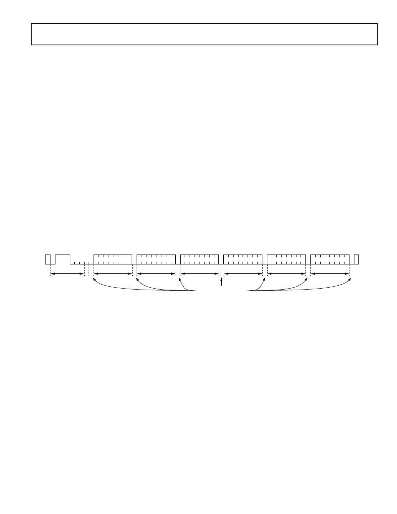
�I� 2� C� Write� Operations�
�A� write� operation� on� the� ADE7953� is� initiated� when� the� master�
�issues� a� start� condition,� which� consists� of� the� slave� address� and�
�the� read/write� bit.� The� start� condition� is� followed� by� the� 16-bit�
�address� of� the� target� register.� After� each� byte� is� received,� the�
�ADE7953� issues� an� acknowledge� (ACK)� to� the� master.�
�As� soon� as� the� 16-bit� address� communication� is� complete,� the�
�master� sends� the� register� data,� MSB� first.� The� length� of� this� data�
�can� be� 8,� 16,� 24,� or� 32� bits� long.� After� each� byte� of� register� data�
�is� received,� the� ADE7953� slave� issues� an� acknowledge� (ACK).�
�When� transmission� of� the� final� byte� is� complete,� the� master�
�issues� a� stop� condition,� and� the� bus� returns� to� the� idle� condition.�
��15�
�8�
�7�
�0�
�23�
�16�
�15�
�8�
�7�
�0�
�7�
�0�
�S� 0� 1� 1� 1� 0� 0� 0� 0�
�P�
�SLAVE� ADDRESS�
�A�
�C�
�MSB� OF� REGISTER� ADDRESS�
�A�
�C�
�LSB� OF� REGISTER� ADDRESS�
�A�
�C�
�BYTE� 3� (MSB)� OF� REGISTER�
�A�
�C�
�BYTE� 2� OF� REGISTER�
�A�
�C�
�BYTE� 1� OF� REGISTER�
�A�
�C�
�BYTE� 0� (LSB)� OF� REGISTER�
�A�
�C�
�K�
�K�
�K�
�K�
�K�
�K�
�K�
�ACK� GENERATED� BY�
�ADE7953�
�Figure� 70.� I� 2� C� Write�
�Rev.� B� |� Page� 53� of� 72�
�发布紧急采购,3分钟左右您将得到回复。
相关PDF资料
EVAL-ADF4002EBZ1
BOARD EVAL FOR ADF4002
EVAL-ADG788EBZ
BOARD EVALUATION FOR ADG788
EVAL-ADM1021AEB
BOARD EVAL FOR ADM1021
EVAL-ADM1023EB
BOARD EVAL FOR ADM1023
EVAL-ADM1031EB
BOARD EVAL FOR ADM1031
EVAL-ADM1062TQEBZ
BOARD EVALUATION FOR ADM1062TQ
EVAL-ADM1075CEBZ
BOARD EVAL FOR ADM1075
EVAL-ADM1087EBZ
BOARD EVALUATION FOR ADM1087
相关代理商/技术参数
EVAL-ADF4001EBZ2
制造商:Analog Devices 功能描述:Evaluation Board For Pll Frequency Synthesizer 制造商:Analog Devices 功能描述:ADF4001 PLL SYNTHESIZER EVAL BOARD
EVAL-ADF4002EB1
制造商:Analog Devices 功能描述:EVAL BOARD - Bulk
EVAL-ADF4002EBZ1
功能描述:BOARD EVAL FOR ADF4002 RoHS:是 类别:编程器,开发系统 >> 评估演示板和套件 系列:- 产品培训模块:Obsolescence Mitigation Program 标准包装:1 系列:- 主要目的:电源管理,电池充电器 嵌入式:否 已用 IC / 零件:MAX8903A 主要属性:1 芯锂离子电池 次要属性:状态 LED 已供物品:板
EVAL-ADF4007EBZ1
功能描述:BOARD EVALUATION FOR ADF4007EB1 RoHS:是 类别:编程器,开发系统 >> 评估演示板和套件 系列:- 标准包装:1 系列:PSoC® 主要目的:电源管理,热管理 嵌入式:- 已用 IC / 零件:- 主要属性:- 次要属性:- 已供物品:板,CD,电源
EVAL-ADF4106EB1
制造商:Analog Devices 功能描述:PLL, Frequency Synthesizer
EVAL-ADF4106EBZ1
功能描述:BOARD EVAL FOR ADF4106 RoHS:是 类别:编程器,开发系统 >> 评估演示板和套件 系列:- 标准包装:1 系列:PSoC® 主要目的:电源管理,热管理 嵌入式:- 已用 IC / 零件:- 主要属性:- 次要属性:- 已供物品:板,CD,电源
EVAL-ADF4108EB1
制造商:AD 制造商全称:Analog Devices 功能描述:PLL Frequency Synthesizer
EVAL-ADF4108EBZ1
制造商:Analog Devices 功能描述:Evaluation Board For ADF4108 制造商:Analog Devices 功能描述:ADF4108 Evaluation Board 制造商:Analog Devices 功能描述:ADF4108, PLL FREQUENCY SYNTHESIZER, EVAL BOARD; Silicon Manufacturer:Analog Devices; Silicon Core Number:ADF4108; Kit Application Type:Clock & Timing; Application Sub Type:PLL Frequency Synthesizer; MCU Supported Families:ADF4108 ;RoHS Compliant: Yes